
Reverse engineering the Van Moof S3 E-shifter
Over the last several years, Van Moof did to electric bikes what Tesla did to electric cars. With their sleek design with integrated battery and kicklock, Van Moof elevated electric bikes to a new level by creating a bike was functional, fast, and easy to ride. Their S3 and X3 models were two of the most high-tech commercial electric bikes at the time they were produced in 2020.
The whole electromechanical system of these bikes comprises many modules, including the electric motor, e-shifter, kick lock, battery and pedal sensor, all of which are connected to a central hub called the smart cartridge. Of all these components, the e-shifter is one of the most notorious of the bike. Many Van Moof owners were (and probably still are) haunted by the ERR 44 displayed when the smart cartridge is unable to communicate with the e-shifter, a fate to which my e-shifter also fell victim. Other times, the gear shift indicator on the display will move back and forth, but the e-shifter does not actually change the gear that the bike is in. There are many electrical and mechanical failure modes that prevent the e-shifter from doing its job of controlling the Sturmey-Archer geartrain and shift gears on command. With a broken e-shifter in hand, I examined the e-shifter, curious to work out how it functions and how it interacts with the smart cartridge, with the ultimate goal to repair my own non-working e-shifter and maybe learning something about reverse engineering.
As a warning to the reader: I'm not an electrical engineer, nor do I have any experience with reverse engineering, so keep that in mind as you read through this post. This is not a guide on how to reverse engineer a component as much as it is a retelling of my experience and a description of what I found going through this process.
Part 1: Electrical investigation
To start on the project, I disassembled my e-shifter and examined its inner workings. The e-shifter consists of a circuit board with several ICs, including a microcontroller, two Hall effect sensors to detect the position of the shifting ring, a motor and motor driver, and various gears to connect the motor to the shifting ring itself. To shift, the smart cartridge communicates via UART with the microcontroller, instructing it to change to the requested gear. The microcontroller then activates the motor in the appropriate direction, rotating the geartrain, which ultimately rotates a gear in the hub itself, changing the gear of the bike.
To start, my first goal was to create an accurate circuit diagram of the PCB. The e-shifter's PCB has two layers, so it is possible to reconstruct the entire circuit schematic by taking high-resolution photos of the circuit board and tracing the connections between components. To do this, I used GIMP, creating paths and regions to annotate traces and copper fill areas on the circuit board. There are a great number of wonderful tutorials on how to do this, so I won't describe my process here. That said, before this project, I had no experience with GIMP at all, but with help from Claude as a tutor, I gained a basic level of proficiency with it. I started with drawing the outlines of all traces and vias on the image onto a separate layer.
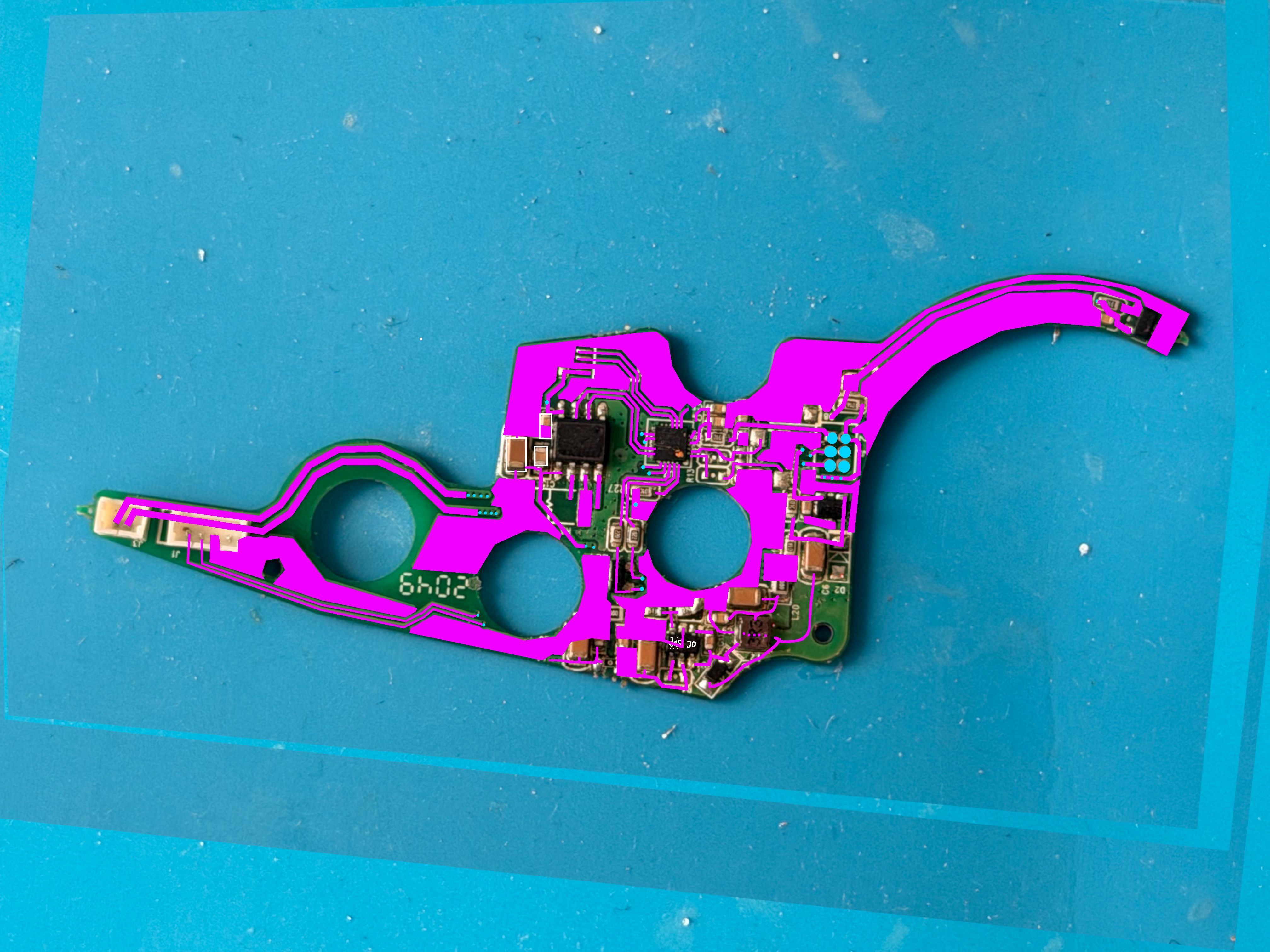
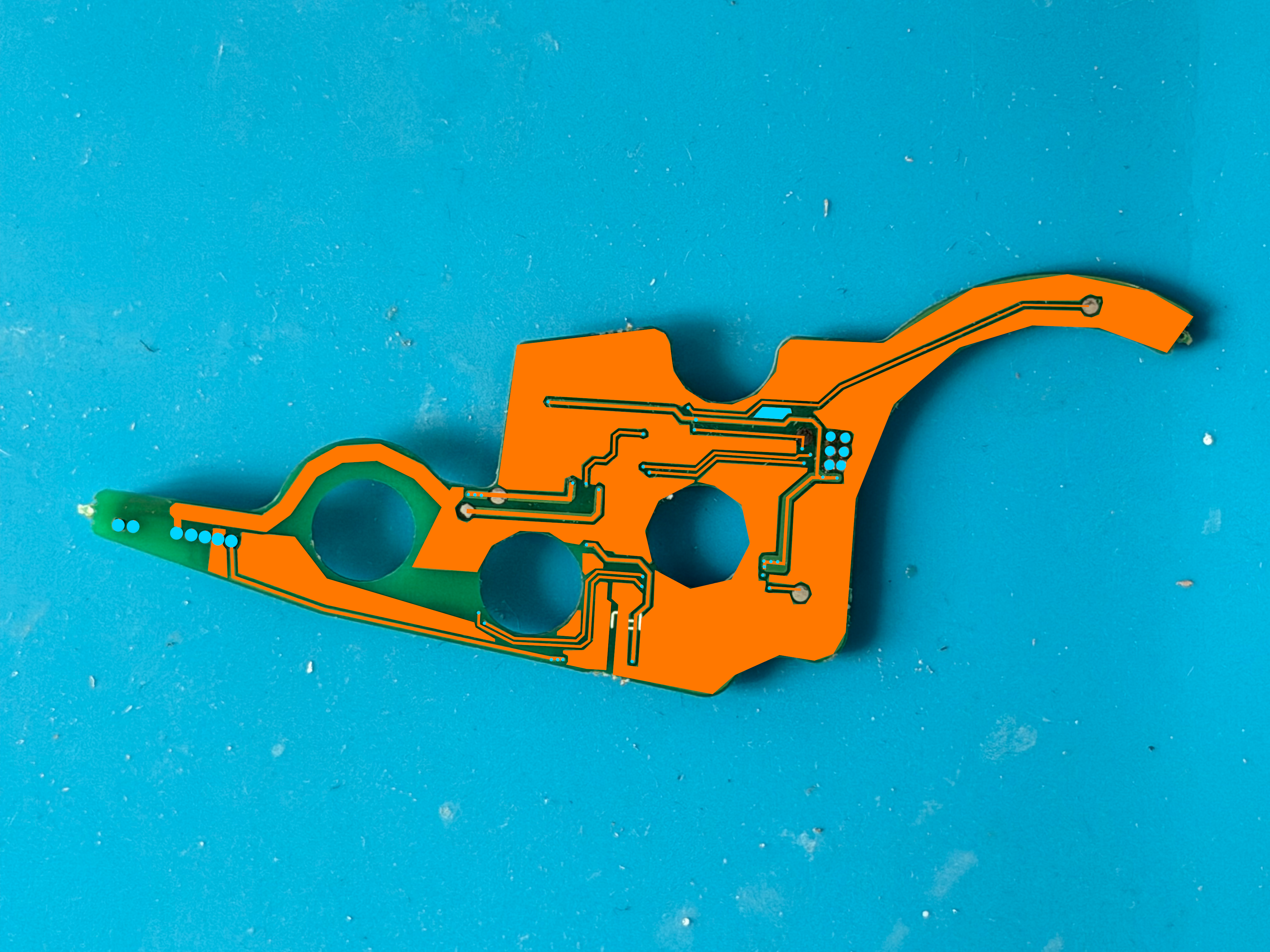
In practice, the images alone are not enough to completely reverse engineer the circuit diagram. A multimeter with continuity mode helps massively to verify whether two components are electrically connected, especially when visibility of the trace is obstructed. In my e-shifter, several traces were routed underneath other components, like underneath the DC-DC driver or the motor driver. I could only confirm those connections with my multimeter.
Alternatively, you can desolder those components from the circuit board using a hot-air gun. However, if you do, be prepared to spend an hour or two painstakingly removing conformal coating. I tried using 99% isopropyl alcohol, scrubbing with a medium-bristle toothbrush, and wiping up the remnants with a lint-free cloth and Q-tips. However, in my experience, much of the coating remained on the circuit board, and I needed to use an Exacto knife or tweezers to carefully remove small bits of conformal coating around the components in question.
Based on these annotated traces, you can then recreate the full schematic. I created all of the components in KiCad and used my trace map to reconstruct the connections between every pair of components.
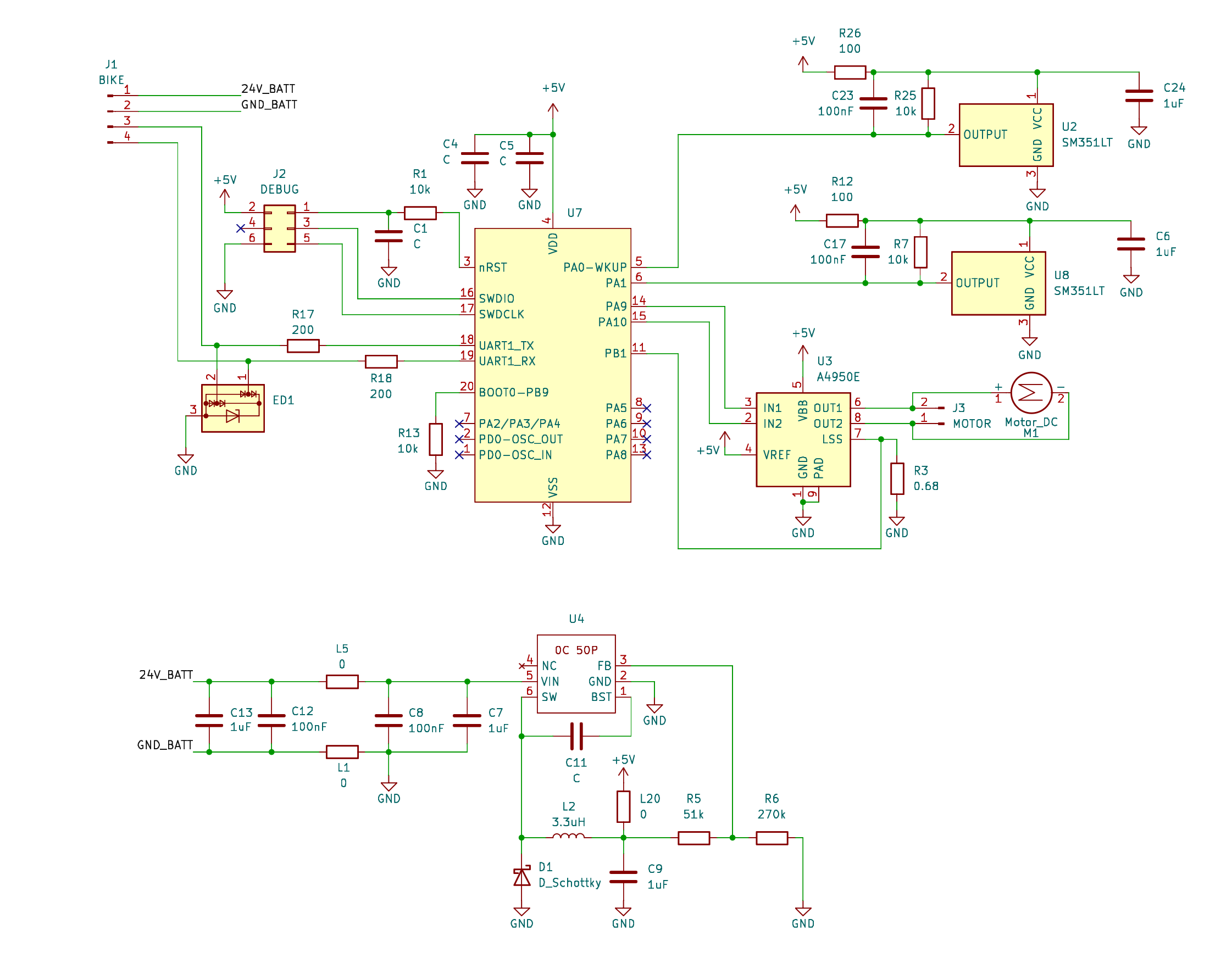
From there, I tested the various components to see if there were any electrical faults. I powered up the motor (which is a 5V brushless DC motor) from my benchtop power supply, and it moved in both directions without a hitch. In my testing, I identified three components with clear faults. The 0-ohm jumper resistor that powers the DC-DC converter sub-circuit had failed open, as did the 680 mOhm sense resistor used by the motor driver to measure the current draw of the motor. Also, a 100 nF capacitor that is part of one of the Hall effect sensors had failed open. I ordered replacement components and placed the new components on my board.
Part 2: Firmware extraction
After fixing the electrical problems, I became very curious about how the microcontroller worked, how it interacted with the various sensors and motor driver, and how it communicated with the smart cartridge. I don't have a spare smart cartridge to use for experimentation, and I wasn't about to sacrifice my S3 for this project, so I wasn't able to snoop on the traffic between the e-shifter and the smart cartridge, like Mike Coats did (this is a wonderful blog and is partially what inspired me to attempt this project). Instead, I took another approach: I would try to recover the e-shifter firmware and analyze the disassembled binary to understand how it works.
First, I had to identify the microcontroller in order to look up its documentation and discover if it even supported some kind of debug protocol. After much searching online, I found that the MindMotion MM32F031F6U6's markings matched those on the chip on my e-shifter. After downloading the data sheet and user manual, I had all the information I would need to continue with the project.
Conveniently, on the board, there is a footprint where a 6-pin connector could be mounted to power and communicate with the e-shifter's microcontroller. Unfortunately, the connector itself is not populated on the production circuit board. However, with help from the data sheet and my schematic from earlier, I worked out that these 6 pins connected to pins on the microcontroller labeled SWDIO, SWDCLK, and nRST, along with VCC and VEE (the 6th pin is not connected).
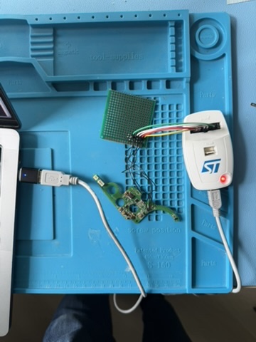
After some googling, I found that these pins are part of the Serial Wire Debug (SWD) protocol, which is used with the STM32 family of microcontrollers. To interact with this debug port, I purchased an ST-LINK/V2 debugger and hacked together a very simple circuit board to connect the e-shifter to the debugger while powering it from my power supply. On my first attempt, I misread the ST-LINK debugger pinout and shorted my VCC and ground connections through my debugger, which wasn't great... after fixing that connection, I was able to use openocd via the ST-LINK debugger to interact with the microcontroller and dump the firmware to my Macbook (the commands of course generated for me by Claude).
Part 3: Bootloader analysis
Now that I had the firmware stored locally, I was ready to try my hand at analyzing it. As this is my first time doing any reverse engineering, I first looked around at open-source software used to disassemble, decompile and annotate binaries. After a brief Google search, I decided that Ghidra would be a suitable software suite for this purpose. I loaded the binary and was presented with 32 kilobytes of assembly code and what seemed like obfuscated C code that Ghidra had reconstructed alongside each detected function.
When importing this binary, I needed to provide the starting memory address used for the storage of the firmware on the microcontroller. This is necessary for memory references, like memory read/write and branching instructions, to resolve to the appropriate place in memory within Ghidra. Unlike your high-level code written in python, where you start on line 1, the firmware is stored in a static memory range. For this MindMotion controller, this 32-kilobyte memory area ranges from 0x08000000 to 0x08007FFF, labeled in the MM32's datasheet as "Main Flash Memory."
However, there are many memory addresses referenced from this code outside of main flash memory, such as registers for configuring the microcontroller or interacting with GPIO pins. Each one of these ranges is described in chapter 4 of the datasheet, Memory Mapping. In Ghidra, references to these memory initially appear in red as a warning to the user that these memory regions are not defined. Each time that the firmware references an address in an undefined memory region, I consulted the datasheet and saw what functionality that region was responsible for, then added a new memory map for that region.
Without any annotation, interactions with memory like this simply appear as load or store instructions to various memory locations. To make more sense of the program's behavior, I defined structures corresponding to the memory layout of the relevant memory locations based on their description in the user guide and the MM32F0160 SDK published by MindMotion. After doing this, the decompiled code shows memory access using user-defined names, which makes it much more interpretable.
One of the main challenges I faced in this firmware analysis was simply figuring out what each function was from its assembly code. For this, I made heavy use of Claude Code. Initially, I copied each function's assembly code from Ghidra into Claude and asked it to tell me what function it was and its function signature. This massively sped up the reverse engineering effort. Claude often identified functions from the MM32 SDK purely from the assembly code and provided me with the appropriate signature. This made function calls much more legible in the decompiled view of the function. However, it also renamed argument registers in the assembly code, which was sometimes even more confusing as one register might be used to store multiple values within a function in addition to the function argument itself.


Ultimately, I was able to deduce the architecture of the e-shifter's firmware. The firmware consists of a bootloader and a main application. The bootloader is responsible for the firmware update process and launching the application itself. The application code is stored in a main memory bank A at 0x08004800, and firmware updates are stored in an auxiliary memory bank B located at 0x08001800. Thus, the firmware can be at most 0x3000, or 12288 in decimal, bytes long. The bootloader only boots the application if bank A is valid and bank B is not. If bank B is valid, it is copied to bank A and then erased and invalidated. If the bootloader receives a message on its UART within 250 milliseconds, it will erase and invalidate bank A and enter into a debugging mode to receive a new version of the firmware.
The approximate pseudocode for the bootloader is:
initialize systick handler
initialize UART1 handler
enable clock for AHB peripherals

if memory bank A header = 0xAA55AA55:
    bank_a_crc <- memory bank A cached CRC
if memory bank B header = 0xAA55AA55:
    bank_b_crc <- memory bank B cached CRC
    if bank B CRC is valid and bank B CRC != bank A CRC:
        copy bank B to bank A
    else:
        erase bank B

wait 250 ms
if UART1 received a MODBUS packet:
    erase bank A and mark invalid

if bank A is valid and bank B is invalid:
    launch the application
else if both bank A and B are valid:
    reset the system
else:
    handle UART commands to load firmware to bank B
One interesting thing I noticed is that the bootloader does not clear memory bank B after copying it to bank A. Instead, the chip is reset, and then because bank's A and B are both valid and the CRC checksums match, bank B is then cleared, and the updated application is launched.
One clever thing about the firmware is that it includes its own checksum inside of it. How does it do this? The checksum is a CRC32 checksum, which occupies 4 bytes of memory and is stored at offset 0x8 in the firmware. When computing the checksum of a memory bank, the bootloader first stores the original value of the checksum, sets this memory region to 0xffffffff, then computes the checksum. I suppose this is a common approach, but I found it clever.
The UART debugging interface was also interesting to work through. However, it shares much in common with the main application's UART interface, so I've described them together below.
Part 4: Application analysis
In order to understand the e-shifter application, we first need to start with the peripherals that the e-shifter interacts with. The e-shifter has two hall sensors, used in two different ways:
- Hall sensor 1 (connected to pin 5, i.e. PA0) changes state each time that one gear passes by it.
- Hall sensor 2 (connected to pin 7, i.e. PA2) is low in first gear and high in higher gears. My understanding is that hall sensor 1 allows the e-shifter to keep track of the current gear. The firmware only notes whether the value for the hall-effect sensor has changed, so the magnetic field polarity for gears 1 and 3 is the opposite of that of gears 2 and 4. Hall sensor 2 is primarily used during the homing process: the homing logic attempts to downshift until hall sensor 1 goes low.
Additionally, it leverages a motor driver, the AT4950TP, an inexpensive brushed DC motor driver. This driver supports a forward, reverse, brake, and coasting mode, but in the e-shifter only the forwards, reverse and brake modes are used. If you've ever opened up your Sturmley-Archer shifter in the Van Moof S3, you may notice that there is no retraction spring that pulls the hub into first gear. Instead, the e-shifter holds the current gear in place using the brake feature while idle.
Now, on to the application itself. The e-shifter application reset handler begins with the C prelude, reconfiguring the clock and initializing its stack, .data and .bss sections, before jumping into the application main function itself. The application has its own prelude, configuring timers and peripherals, copying its vector table to SRAM and reconfiguring the Cortex-M0 core to use that vector table, and reloading its own state persisted to flash.
It seems like the e-shifter I analyzed has an older firmware, dating back to late 2020:
        08004810 4f 63 74        ds         "Oct 23 2020\014:09:11"
                 20 32 33
                 20 32 30
After that, the e-shifter main application begins. It can be described wit the following pseudocode:
relocate vector table & configure memory remap
enable clock for AHB/APB1/APB2  # needed for FLASH/CRC, TIM2, UART1 respectively
configure GPIO
configure UART
load persisted state
initialize shifter
cache hall 1 value
last_loop_iteration_ms <- current time milliseconds
while true:
    last_shifter_state <- load last shifter state
    handle any request received on UART1
    drive the e-shifter motor and detect timeouts
    if current time milliseconds < last_loop_iteration_ms:
        last_loop_iteration_ms <- current time milliseconds
        handle last_shifter_state
The main loop and e-shifter state handler are both written as event loops, and there is no sleep or delay of any kind in the main loop. Instead, control flow will repeatedly progress down the same pathway on each loop iteration. The time in milliseconds is cached when an action is started, and the current time is checked on each iteration of the loop to track how long an operation has taken place (such as the motor running for a certain duration). The e-shifter state handler is only invoked once per millisecond, so it is possible for the e-shifter to communicate with the smart cartridge multiple times before the e-shifter handles its own state.
The e-shifter state has 7 different values:
| Name | Value | Comment |
|---|---|---|
| SystemMode_Reset | 0 | Clear the shift count, reset current gear to 1. |
| SystemMode_NeedsHoming | 1 | Trigger the homing routine to ensure the gear ring is at the expected position. |
| SystemMode_Normal | 2 | Normal operation. |
| SystemMode_HomingTimeoutGear1 | 3 | The homing routine timed out near gear 1. |
| SystemMode_HomingTimeoutGear4 | 4 | The homing routine timed out near gear 4. |
| SystemMode_HomingTimeoutGears23 | 5 | The homing routine timed out between gears 2/3. |
| SystemMode_Fault | 6 | The shifter was unable to rehome or complete a shift within the allowed number of retries. |
In general, the e-shifter starts by rehoming itself unless it is sure that it is in first gear. The homing process is fairly straightforward: the e-shifter simply downshifts until the hall 2 sensor is inactive. Once that happens, the motor is stopped, and the e-shifter persists that it is in first gear. There is one subtlety to this: if the homing routine times out before hall sensor 2 reads low but the shifter is in first gear, the shifter enters state SystemMode_HomingTimeoutGear1 and actually advances the shifter forward with a shorter timeout until second gear is entered, thereafter attempting to going back down to first gear.
Under normal circumstances, the e-shifter sets the motor in the appropriate direction and counts the gears passing by Hall effect sensor 1. Once the correct number of gears have passed, the e-shifter leaves the motor running for a few more milliseconds, depending on the gear and direction of shifting. These extra durations are presumably empirically computed based on the geometry of the shifter, position of the magnetic field along the gear ring, the sensitivity of the Hall effect sensor, and potentially backlash in the shifting system.
In either the homing case or the shifting case, a timeout may be reached before the target gear is reached. In that case, the e-shifter records that by setting a secondary mode variable. This motor submode captures similar cases to the main system state enum above.
| Name | Value | Comment |
|---|---|---|
| MotorSubmode_Idle | 0 | The e-shifter is idle. |
| MotorSubmode_HomingActive | 2 | The e-shifter is homing and close to first gear. |
| MotorSubmode_ShiftTimeoutFarFromGear1 | 3 | The e-shifter timed out while shifting, and the current gear is not close to first gear. |
| MotorSubmode_HomingTimeoutGear4 | 4 | The e-shifter timed out while homing near fourth gear. |
| MotorSubmode_HomingTimeoutGear23 | 5 | The e-shifter timed out while homing in either second or third gear. |
| MotorSubmode_ShiftTimeoutNearGear1 | 6 | The e-shifter timed out while shifting while close to first gear. |
| MotorSubmode_HomingNeeded | 7 | The e-shifter needs to start homing. |
| MotorSubmode_Fault | 8 | The e-shifter has not successfully shifted or homed within the max allowed attempts. |
The e-shifter keeps track of whether shifting or homing failed close by first gear. The main difference that this has on the firmware is that it reduces the motor timeout from 2 seconds to 200 milliseconds for motor operations. I guess that this is done to reduce the chance of damaging components by overdriving the gear ring, but I'm not very sure about this.
Part 5: Communication Protocol
Both the application and the bootloader support a communication protocol with the smart cartridge. This protocol is based on the Modbus over RS-232, with a frame consisting of a slave address, a command, either 4 or 41 data bytes, and a two byte little-endian CRC16 checksum.
The short message is used for all communication aside from firmware chunk transfers. The interpretation of the 4 data bytes depends on the value of the second byte (index 3 into the frame itself), which I'll call the operation.
The bootloader UART loop supports 4 operations:
| Operation | Command | Description |
|---|---|---|
0x01 |
0x3 or 0x6 |
Echo. Always returns 20 03 02 02. |
0x81 |
0x3 or 0x6 |
Verify memory bank B CRC. |
0x82 |
0x10 |
Write a 32-byte chunk of firmware to memory bank B. |
0x95 |
0x3 or 0x6 |
Clear memory bank B. |
This allows a user to update the e-shifter application firmware via a debugging interface without needing to connect physically to the SWD interface. However, the bootloader itself cannot be modified via this mechanism.
The application UART loop is much more extensive. Several operations appear to read static values that were programmed into the firmware, the meaning of which I'm not able to deduce purely from looking at one version of the firmware itself. These values are stored in address range 0x200000eb-0x200000f4. For simplicity, I'll name this region FIRMWARE_CONFIG. These values are statically allocated and are copied as part of the C runtime setup. Some other statistics are persisted in flash directly in the page starting at 0x08007800, which I call STATS.
Also, for several commands, byte 5 of the request includes a transaction or request ID, which I've abbreviated as RID. This value is included as the first data byte in the response, left shifted by 1 bit. I'll call this LSRID for left-shifted request ID. The response always begins with the same first two bytes as the request (i.e. 0x20, the static client address of the e-shifter, and the specified command byte), so for brevity I omit those from the response description. Likewise, the last two bytes are the little-endian CRC16 checksum of the message.
| Operation (request byte 3) | Command | Description | Request data | Response data |
|---|---|---|---|---|
| 0x0 | N/A | Return FIRMWARE_CONFIG[0] and FIRMWARE_CONFIG[1]. |
5: RID |
2: LSRID 3: FIRMWARE_CONFIG[0] 4: FIRMWARE_CONFIG[1] |
| 0x1 | N/A | Return FIRMWARE_CONFIG[2] and FIRMWARE_CONFIG[3]. |
5: RID |
2: LSRID 3: FIRMWARE_CONFIG[0] 4: FIRMWARE_CONFIG[1] |
| 0x2 | 0x3 | Read the current gear index. | 5: RID |
2: LSRID 3: 0 4: current gear |
| 0x2 | 0x6 | Set the gear to the requested value. | 5: requested gear | echo the request data exactly |
| 0x3 | N/A | Read the motor secondary mode value. | 5: RID |
2: LSRID 3: 0 4: current motor submode |
| 0x4 | N/A | Echo. | 5: RID |
2: LSRID 3: 0 4: 0 |
| 0x5 | N/A | Return FIRMWARE_CONFIG[6] and FIRMWARE_CONFIG[5]. |
5: RID |
2: LSRID 3: FIRMWARE_CONFIG[6] 4: FIRMWARE_CONFIG[5] |
| 0x6 | N/A | Return FIRMWARE_CONFIG[8]. |
5: RID |
2: LSRID 3: 0 4: FIRMWARE_CONFIG[8] |
| 0xd | N/A | Return FIRMWARE_CONFIG[10]. |
5: RID |
2: LSRID 3: 0 4: FIRMWARE_CONFIG[10] |
| 0xf | N/A | Return the total shift count. | 5: RID |
2: LSRID 3: 0 4: FIRMWARE_CONFIG[10] |
| 0x14 | N/A | Trigger homing if motor is not active. | N/A | N/A |
| 0x5a | N/A | Engage the motor if motor is not active. | 5: Motor direction | N/A |
| 0x5b | N/A | Read the hall sensors. | 5: RID |
2: LSRID 3: 0 4: one of 0, 0x32, 0x64, or 0x96 |
| 0x5c | N/A | Update firmware stats. | 2: Stats byte 6 4: Stats byte 7 5: Stats byte 8 |
N/A |
| 0x81 | N/A | Finalize firmware update: verify memory bank B and trigger reset. |
5: RID |
2: LSRID 3: 0 4: 0 (CRC match), 1 (CRC mismatch), 2 (missing magic) |
| 0x82 | 0x10 | Copy firmware bytes to flash memory. | 11-43: firmware chunk | 0-5: first 6 bytes of request |
| 0x95 | N/A | Erase memory bank B and activate long-message mode. |
N/A | N/A |
Part 6: Retrospective
SRAM Reuse. One thing that makes this analysis quite challenging is that the bootloader and application reuse the same areas of SRAM for different purposes. For example, address 0x200000c4 holds the UART1 buffer length while the bootloader is active, but later on during the application, this memory address stores a timer which is decremented each time the SYSTICK interrupt fires. The same address can even hold different data types or be aliased in different ways based on this distinction. So I would advise doing analyzing the bootloader and application in separate analysis passes, and when doing so, clear the analyzed bytes of the opposite part so that the automatically added references don't pollute the Ghidra UI.
Unidentified memory. Interestingly, there were still memory regions from the original firmware that Ghidra did not recognize as instructions, nor were referenced from any code. I never understood what these regions were used for in the firmware, as they seemed never to be referenced from anywhere.
LLM tools helped tremendously. I made heavy use of Anthropic's Claude throughout this project, both for guidance on how to use GIMP and Ghidra, as well as helping directly with identifying library functions from the MM32 SDK and understanding the behavior of the custom bootloader and main application. Taking on a project of this scale would have been far beyond my ability without the help of LLM tools. That said, these tools were not perfect, and over time I felt like I was able to analyze the program faster using Claude sparingly (and it was more fun that way too). I did not use any such tools when writing this blog post, however.
Ghidra complexity. I found some aspects of how Ghidra relates disassembled and decompiled code to each other quite confusing. When naming a register-based variable in the decompiled view, Ghidra takes the liberty to rename the corresponding register in the disassembled view of the function. However, the data in registers is frequently moved to other registers. For example, a function argument may need to be moved to another register so that a different argument can be passed to a different function. The result is that the register's annotated name may be correct in some parts of the function and misleading in other parts. This happens presumably because Ghidra doesn't know whether an assignment to the same register represents updating the value of that register or replacing that register's value with an entirely different variable. To address this, you need to use the "Split out as new variable" context menu operation from the decompiler window. This creates a new variable in the decompiler and correctly updates the decompiled and disassembled views, but it is again difficult to see what the underlying register is. To do this, you double click on the reference name, which brings you to the top of the function and out of the context of where you were before.
Switch statement analysis. Though I was able to analyze dense switch statements from the e-shifter manually, I was not able to successfully decompile these in Ghidra. Such statements have the form:
                             Handle state_0fc (switch table is offset based on state value)
                             State handler is triggered once per millisecond
        08005b88 23 00           movs       r3,r4
        08005b8a 01 f0 13 fd     bl         __switch_table_dispatch                          undefined __switch_table_dispatc
        08005b8e 07              db         7h
        08005b8f 05              db         5h
        08005b90 08              db         8h
        08005b91 19              db         19h
        08005b92 3f              db         3Fh
        08005b93 46              db         46h
        08005b94 50              db         50h
        08005b95 5a              db         5Ah
        08005b96 5e              db         5Eh
        08005b97 00              db         0h
                             state_0fc_0_handler
        08005b98 ff f7 8f f9     bl         reset_state                                      void reset_state(void)
        ...
where an index is put into register r3, and then control flow jumps to __switch_table_dispatch, which has the following structure:
                             **************************************************************
                             *                          FUNCTION                          *
                             **************************************************************
                               undefined __stdcall __switch_table_dispatch(void)
             undefined         <UNASSIGNED>   <RETURN>
                             __switch_table_dispatch                         XREF[2]:     uart1_handle_command:080054b0(c),
                                                                                          app_main:08005b8a(c)
        080075b4 30 b4           push       {r4,r5}
        080075b6 74 46           mov        r4,lr
        080075b8 64 1e           subs       r4,r4,#0x1
        080075ba 25 78           ldrb       r5,[r4,#0x0]
        080075bc 64 1c           adds       r4,r4,#0x1
        080075be ab 42           cmp        r3,r5
        080075c0 04 d3           bcc        switch_argument_overflow
                             jump_to_case                                    XREF[1]:     080075ce(j)
        080075c2 63 5d           ldrb       r3,[r4,r5]
        080075c4 5b 00           lsls       r3,r3,#0x1
        080075c6 e3 18           adds       r3,r4,r3
        080075c8 30 bc           pop        {r4,r5}
        080075ca 18 47           bx         r3
                             switch_argument_overflow                        XREF[1]:     080075c0(j)
        080075cc 1d 46           mov        r5,r3
        080075ce f8 e7           b          jump_to_case
This is not really a function in the traditional sense. Instead, it computes jump_table[r3 + 1] * 2 + &jump_table, where jump_table is the array of 10 bytes immediately following the bl __switch_table_dispatch instruction. This was not recognized as a switch statement by any auto-analysis routines in Ghidra. I think there are three issues that cause the switch statement detection not to work well:
- the traditional switch statement detection tools seem to assume that the offsets in the
jump_tableare byte offsets, but in this case, they are two-byte offsets. - the dispatch function is not inlined, so the indirect jump (
0x080075ca) is shared between all switch statements; what varies is thelrregister which provides this routine with the jump table address.
I attempted several mitigations:
- changing the call fixup of the
__switch_table_dispatchtoswitch8_r3as recommended here - adding COMPUTED_CALL references to the indirect jump instruction
- adding COMPUTED_CALL references to the
bl __switch_table_dispatchinstruction - changing the instruction flow type of the
bl __switch_table_dispatchinstruction toBRANCH
Modifying the instruction flow type was the only option that changed the decompiled code, but under no circumstance was the switch statement generated by the decompiler.
Part 7: Conclusion
You might ask me, what was the good of this project? Did I even fix my e-shifter? What do I plan to do with this newfound knowledge about the e-shifter? Honestly, you'd probably be disappointed to hear that this is where I'm stopping with this project. I did fix the e-shifter electrically, but the plastic case was destroyed. I'm not going to build my own bootloader or custom firmware or redesign the e-shifter circuit board or anything like that. However, I feel like I'm now armed with some amazing tools for taking on other projects like this in the future. More importantly, I have more confidence in myself and my ability to take on a substantial project like this. I dealt with many ambiguities and open questions, nor I wasn't following a step-by-step guide. It feels like I leveled up my problem solving skills a notch or two in this project, and I look forward to the next project when I can build on top of these skills again.